Research Centers
Internet of Things Centre
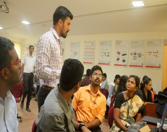
About this Lab
The ECE – IoT CENTRE were established on 2017, dedicated to create a platform to interact with other educational institutions and industrial forum for research and development and focus on use cases and build reusable assets in IoT space. Karunya ECE-IoT centre serves as a forum for budding engineers to simulate, design, develop use cases in RFID technology, camera based image identification, analysis and optical recognition (OCR), industrial sensors and support the standard integration and communications protocols such as Wi-Fi, Bluetooth and LoRaWAN for industrial automation.
Hardware Equipments
- LoRaWAN Multi channel outdoor Gateway(DL0S8)
- IoT- LoRaWAN WDM boards
- IoT- LoRaWAN Shields
- Raspberry pi Development boards
- ESP32 development boards
- Intel Edison Development board
- NI Myrio board
- TM4C129E Crypto Connected IoT Gateway
- CC2650 Sensor tag
- CC3200 WIFI
- CC110L RF
- MSP432
- Industrial Sensors
- MSP430
Software Tools
- Arduino IDE
- Raspberry pi – Raspbian OS
- Energia IDE
- NI Myrio LabVIEW
Certificate Courses
Machine learning with python programmingHands on training using Arduino IDE and Arduino development boardsHands on training on IoT using Raspberry pi development boards Training Program on IoT development boards with LoRaWAN TechnologyHands on training on IoT using ESP32 development boards
Testing Services
Real time Data monitoring using The Things Network (TTN) cloud platformReal time sensor Data Acquisition LoRaWAN Nodes and LoRaWAN outdoor gateway
Courses Offered
IoT for Communication Engineering Laboratory (20EC2006)Building automations systems Laboratory (20EC2016)Electronics for intelligent machines Laboratory (20EC1005)IoT Projects
LoRA WAN Outdoor gateway 868 MHzRange -> 5 to 7 Km 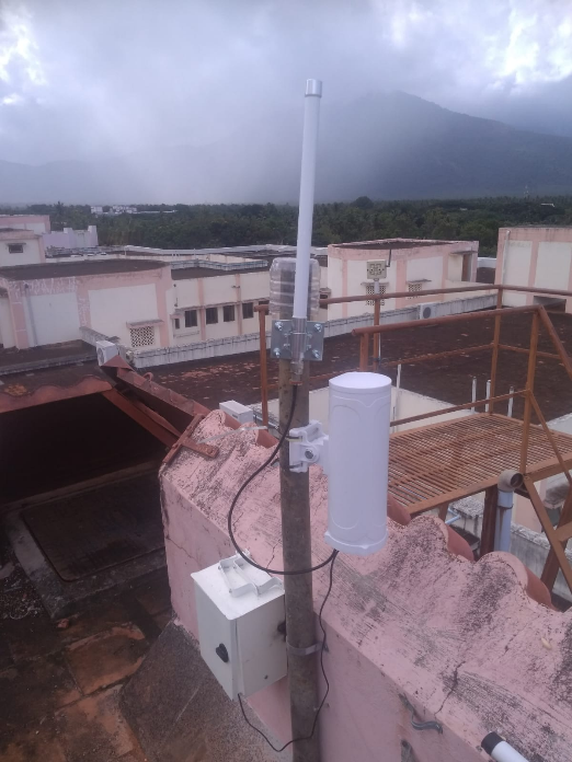
Industry Support


Contact Details
Industry Support
Faculty in-charge : Mr. J. John Paul, Asst. prof [email protected]Staff incharge : Mr. M. Wilson Christopher Raj[email protected]Lab Intercom : 0422-2614393(4187)
Centre of Excellence in VLSI Design
Karunya has signed MoA with M/s Test and Verification Solutions India Pvt Ltd on Jan 2019. As part of MoA, a centre is established and students are provided with industrial training and real time projects to be technically equipped.
This centre is established to carry out semiconductor device fabrication and modeling in the current micro and nano scale level. Collaborative research projects with Department of Space (ISRO), Ministry of Defence (DRDO) and Department of Electronics and are carried out in this lab.

ABOUT THE CENTRE
The centre of Research in Semiconductor Devices was established in the Department in the year 2019. This centre is established to carry out semiconductor device fabrication, simulation and modeling in the current micro and nano scale level to meet Industrial needs. Collaborative research projects with Department of Space (ISRO), Ministry of Defence (DRDO) and Department of Electronics are carried out in this centre. Centre of Research in Semiconductor Devices
FACILITIES
Hardware Equipments
- DC Sputtering Unit (Thin Film Physical Vapor Deposition Coating technique - PVD).
- Pelletization (Compressing or molding materials into Pellet Shape).
- Silicon wafer (N type, P type).
- Substrate (Glass).
- Target (Copper, Silver, Molybdnum)
Software Tools
- Synopsys TCAD Asiapac Advanced.
- Silvaco – TCAD OMNI Bundle.
SPONSORED PROJECTS
| Title of the Project | A Compact modeling of GaN based HEMT device for high power microwave applications |
| Grant | 21.98 Lakhs |
| Funding Agency | DRDO |
| Duration | 2017-2019 |
| Title of the Project | Design and Fabrication of Case-Code driver circuit using GaN HEMT on Si for space applications |
| Grant | 30.44 Lakhs |
| Funding Agency | ISRO |
| Duration | 2019-2022 |
Visvesvaraya PhD Scheme
Mrs.D.Gracia (Research Scholar) is receiving a scholarship of Rs.31, 500 per month under Visvesvaraya Ph.D. Scheme for Electronics and IT launched by Department of Electronics and Information Technology (DeitY), Ministry of Communication and Information Technology, Government of India for the funded project “Tunnel FET for Low Power Applications”.
SELECTED PUBLICATIONS
- A.S. Augustine Fletcher, D. Nirmal, L. Arivazhagan, J. Ajayan and Varghese, A, "Enhancement of Johnson figure of merit in III-V HEMT combined with discrete field plate and AlGaN blocking layer", International Journal of RF and Microwave Computer-Aided Engineering,vol 30, Issue 2(2020).
- K.Husna Hamza and D. Nirmal, "A review of GaNHEMT broadband power amplifiers", International Journal of Electronics and Communications (AEU), Vol 116, (2020) DOI:10.1016/j.aeue.2019.153040 .
- D.Godfrey, D.Nirmal, D. Godwinraj L. Arivazhagan,N.Mohankumar,J.Tzou and W.K.Yeh "Enhancement of DC and Breakdown Performance on Single to Multi-Step, Gate FP Using GaN-HEMT for High Power Applications", Silicon DOI: 10.1007/s12633-020-00503-4(2020).
- Ravindran, A., Nirmal, D., Prajoon, P., Gracia Nirmala Rani, D ,Optical Grating Techniques for MEMS-Based Spectrometer - A Review, .IEEE Sensors Journal, 2021, 21(5), pp. 5645–5655, 9272803, DoI: 10.1109/JSEN.2020.3041196
- Ajayan, J., Nirmal, D., Mathew, R., ...Arivazhagan, L., Ajitha, D , A critical review of design and fabrication challenges in InP HEMTs for future terahertz frequency applications, Materials Science in Semiconductor Processing, https://doi.org/10.1016/j.mssp.2021.105753, 2021, 128, 105753
- Husna Hamza, K., Nirmal, D., Augustine Fletcher, A.S., Arivazhagan, L., Ajayan, J., Natarajan, R., Highly scaled graded channel GaN HEMT with peak drain current of 2.48 A/mm (2021) AEU - International Journal of Electronics and Communications, DOI: 10.1016/j.aeue.2021.153774
- Anvarifard, M.K., Nirmal, D. Creation of Step-Shaped Energy Band in a Novel Double-Gate GNRFET to Diminish Ambipolar Conduction (2021), IEEE Transactions on Electron Devices, DOI: 10.1109/TED.2021.3069442
CONSULTANCY
- Device Design
- Fabrication and Testing
INDUSTRY SUPPORT
Contact Details
| Faculty in-charge | |
| Staff in charge | |
| Lab Intercom | 0422-2614393(4139) |