Welcome to 5th International Conference on Devices, Circuits and Systems (ICDCS'20)
5th IEEE International Conference on Circuits, Devices and Systems
KEYNOTE- 1 |
|
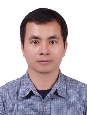
Transistor 70, IC 60, and next? Dr. Wen-Kuan Yeh, Professor, Electrical Engineering Department, National University of Kaohsiung |
|
Abstract: As CMOSFETs are scaled down to 3nm and below, power consumption is the major limitation to maintain device performance well. Thus, how to suppress the device’s sub-threshold leakage and gate leakage is the key issue for sub-5nm CMOSFET especially for high performance/lower power system. In order to scale CMOSFET following Moore’s law continuously, there are some candidates are introduced to replace conventional MOSFET structure including GAAFET, TFET, NCFET and 2D material FET. This talk will explain semiconductor device trend and related advanced technology development especially for coming 3nm technology regime. Heterogeneous Integration was proposed for keeping Moore’s law with scaling transistor. And other specific device for more than Moore application including sensor, energy harvesting device for Internet on Thing (IoT) will be also explained. |
|
KEYNOTE- 2 |
|
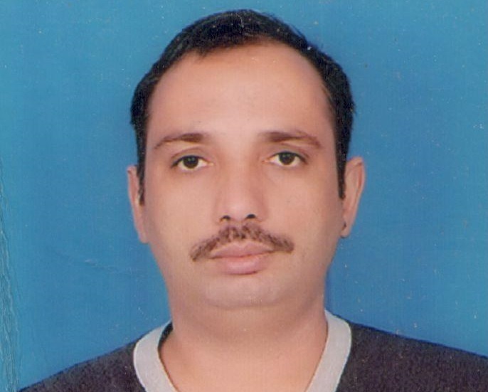
GaN on Silicon Manufacturing Excellency in CMOS foundary Dr Manish Kumar Hooda, Professor, Head - Technology Development Division, Semi-Conductor Laboratory, Department of Space, Govt. of India Mohali. |
|
SHORT BIO Dr Manish Kumar Hooda has done his Masters in Electronics with specialization in Microelectronics. He Received his Ph.D. in Microelectronics from Kurukshetra University, Kurukshetra, India. He has started his carrier as a VLSI design Engineer at ST Microelectronics followed by Associate Scientist at CSIO Chandigarh. He joined I.S.R.O. (SCL) in 2004 since then he has been working on development of fabrication processes for VLSI ASIC, MEMS/NEMS devices. He has been responsible for Process Integration for various VLSI ASICs, MEMS/NEMS devices. He has a research experience of more than 18 years In VLSI, MEMS and ASIC Fabrication & Process Integration. He has a hands on experience of handling of almost all type of micro fabrication equipment's being used in Wafer fabrication industries like (KOH Bulk Micro-machining, Surface Micro-machining, Dry Etchers (Dielectric, Metal and Poly etcher) thin film deposition tools, Sputter Tool, Wafer Bonder, Diffusion Furnaces, LPCVD tools, PECVD and Deep Reactive Ion Etching tools. He has published 30 research papers in various National and international Journals. He has guided six Ph.D students.. His research Area is focused on Development of MEMS and NEMS Devices for Micro-propulsion Systems for Space and Bio Medical Applications, Device Development based on Hetrostructures HEMTs, Power Devices, optical devices based on III-V compound Semi-conductors on Silicon. Presently, he is responsible for developing and augmenting new Semiconductor Technologies required for India's future Space and strategic programme. |
|
KEYNOTE- 3 |
|
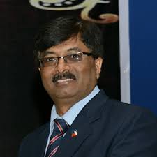
Dr. D. S. Rawal, Associate Director, SSPL, Delhi. |
|
SHORT BIO Dr. D. S. Rawal is an Associate Director at Solid State Physics Laboratory (SSPL), Delhi, working in the area of III-V Device Technology. He joined SSPL, Delhi in 1992 and has mainly worked for the development and Transfer of Technology of GaAs MMIC technology that is presently undergoing production at GAETEC, Hyderabad. He received his M.Sc. Degree in Physics and M.Tech. Degree in Electronics and Communication Engineering from University of Roorkee, Roorkee, India (Now IIT Roorkee), in 1988 and 1990, respectively. He did his PhD in Experimental Plasma Physics from IIT Delhi. Presently, he is heading Fabrication team at SSPL Delhi for the development of GaN based MMIC Technology. He has published more than 70 research papers in various international journals and conferences. He is also an active reviewer for various reputed international journals like Applied Surface Science (Elsevier), JVST A/B (AIP), IEEE trans. on Semiconductor Manufacturing, IEEE Sensors, Surface Coating and Technology (Elsevier), Vacuum (Elsevier), Journal of Alloy and Compounds (Elsevier), Nanotechnology (IOP science) and Journal of Physics D (IOP). He has many awards to his credit and is a recipient of DRDO Path Breaking Research Award (Twice), Scientist of the Year Award and Elsevier Outstanding Reviewer Award etc.
|
|
ICDCS'20
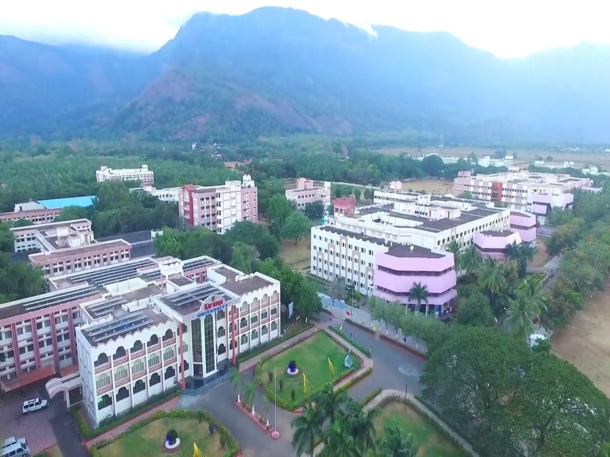
The venue for the conference is
Department of Electronics and Communication Engineering, Karunya Institute of Technology and Sciences, Coimbatore